Abb+ufes+manual Jun 2026

Compatibility:

abb+ufes+manual

OptiFDTD

70 MB

Below are popular user links:

FDTD Publications
FDTD Videos
FDTD Features
FDTD Tutorials

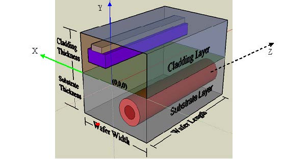
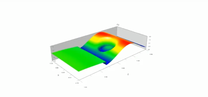
OptiFDTD enables you to design, analyze and test modern passive and nonlinear photonic components for wave propagation, scattering, reflection, diffraction, polarization and nonlinear phenomena. The core program of OptiFDTD is based on the Finite-Difference Time-Domain (FDTD) algorithm with second-order numerical accuracy and the most advanced boundary conditions – Uniaxial Perfectly Matched Layer (UPML).

The algorithm solves both electric and magnetic fields in temporal and spatial domain using the full-vector differential form of Maxwell’s coupled curl equations. This allows for arbitrary model geometries and places no restriction on the material properties of the devices.

Applications

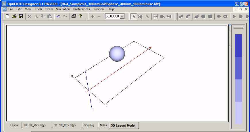
  • Surface Plasmon Resonance (SPR)
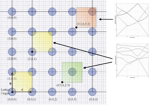
  • Photonic band gap materials and devices
  • Nano-particles, and tissue cells
  • Diffractive micro-optics elements and lenses
  • Complex integrated optics structures
  • Nonlinear materials, dispersive materials
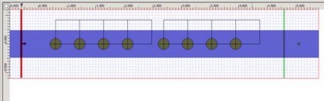
  • Optical micro-ring filters and resonators
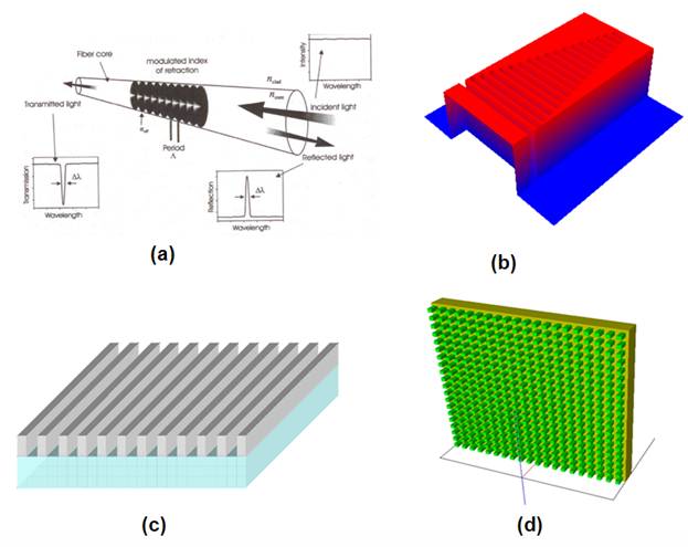
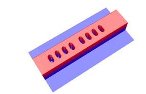
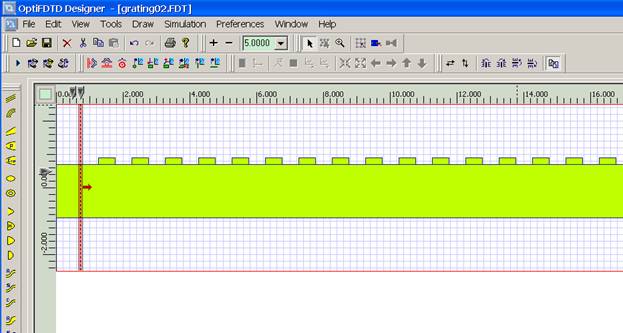
  • Grating based waveguide structures
  • Electromagnetic phenomena


Interface with Popular DesignTools
  • Code V
  • Zemax

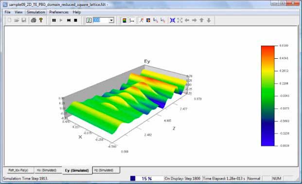
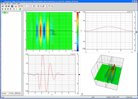
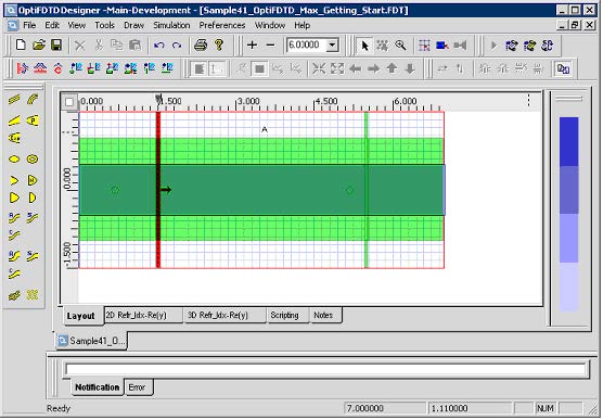
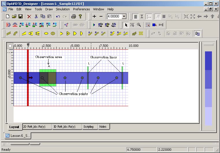
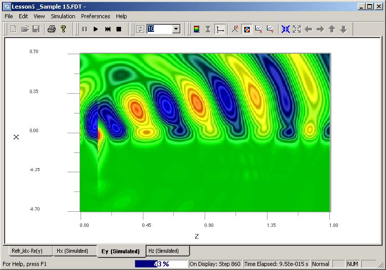
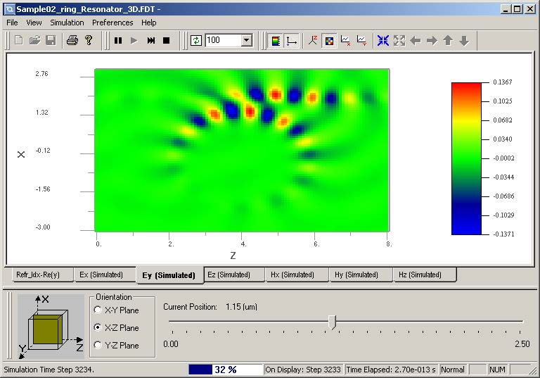
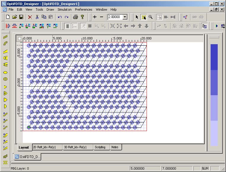
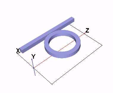
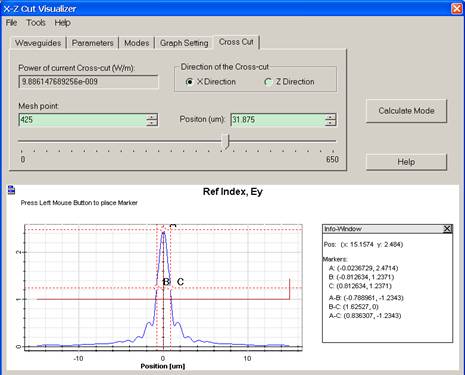
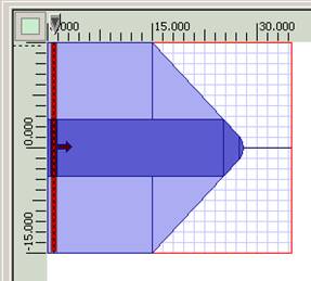
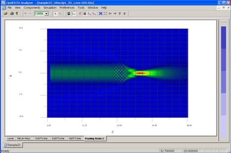
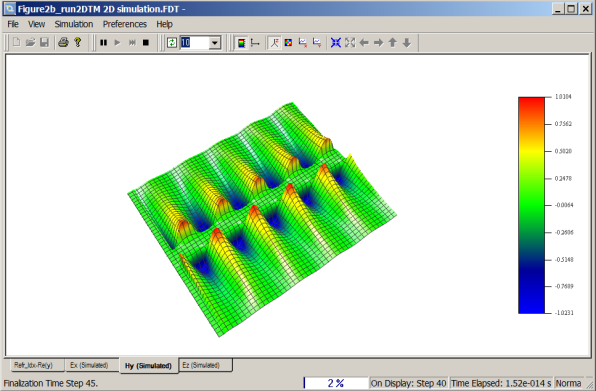
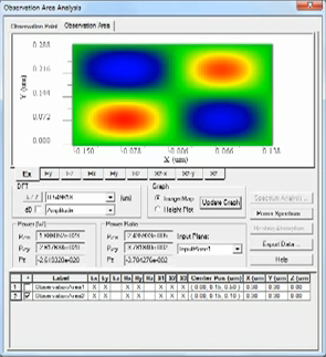
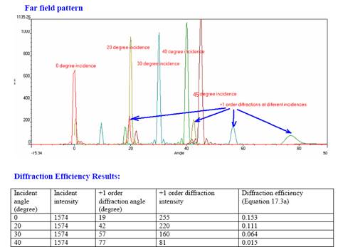
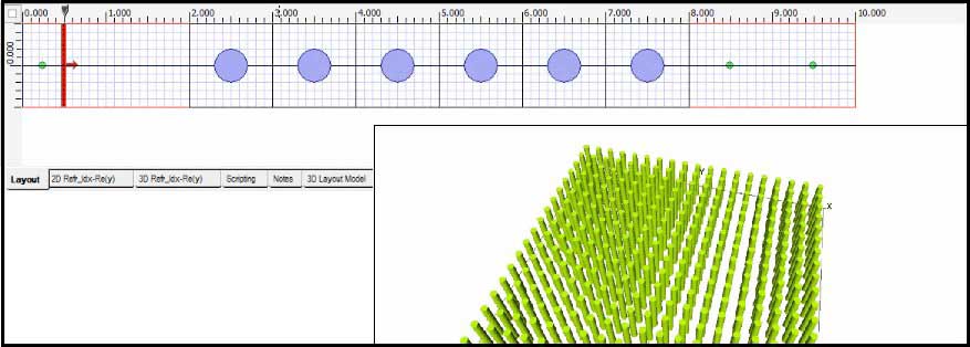
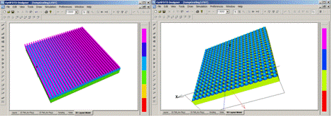
Feel free to browse our FDTD gallery (click to enlarge):

     FDTD - Figure 3 Inversion Symmetry and Domain Origin FDTD - 3D Wave propagation

FDTD - Figure 8 The time domain snapshot observed in 3D Viewer from observation area 2FDTD - Figure 5 Layout

FDTD - Figure 16 Elliptic waveguide in the TFSF regionFDTD - Figure 2 Layout in OptiFDTD

FDTD - Figure 10 Observation components of projectFDTD - Selected Grating layout

FDTD - Figure 2 Example LayoutFDTD - Figure 1 3D layout mode for sphere

  FDTD - Observation Area Analysis dialog box FDTD - Figure 106 Observation Area Analysis dialog box

FDTD - Figure 5 OptiFDTD_Simulator FDTD - Figure 40 3D Simulation results

FDTD - Figure 95 PBG layout with new wavepath FDTD - Figure 18 3D Layout

FDTD - Beam size measurement in OptiFDTD(b)

FDTD - Poynting vector for Fiber lens  FDTD - Surface wave propagation model

FDTD - Power transmission ratios and normalised powersFDTD - Near field in slice viewer

FDTD - Photonic Crystal Layout FDTD - Diffraction Grating 3D Layouts

Layout in OptiFDTD  Directional grating Coupled waveguide in OptiFDTD

Layout in OptiFDTD  FDTD - Nanoparticle plane wave and the nanoparticle intensity

Related:

Abb+ufes+manual Jun 2026

The system continuously monitors for light (via lens or fiber sensors) and instantaneous current.

ABB UFES (Ultra-Fast Earthing Switch) is an active arc fault protection system designed to extinguish internal arcs in medium-voltage switchgear in less than 4 milliseconds abb+ufes+manual

UFES (Universal Fieldbus Engineering System) is ABB’s engineering toolset for configuring, commissioning, and maintaining fieldbus networks and devices used in industrial automation. It supports protocols like PROFIBUS, FOUNDATION Fieldbus, DeviceNet, and CANopen (depending on ABB product integrations) and helps integrate ABB field devices (valves, drives, sensors, I/O modules) into control systems. The system continuously monitors for light (via lens

: PSEs can be installed in cable connection compartments or on busbar sections. : PSEs can be installed in cable connection

: The primary switching elements (PSE) have an extremely short switching time of less than Electronic Control Units